semiconductor manufacturing
Markets

Semiconductor

Minuscule dimensions. Monumental impact.
Semiconductor

Semiconductor

The future of semiconductor design and manufacturing is increasingly intertwined with advancements in precision optics, which are essential for continued miniaturization and enhancement of chip performance. 

The ultimate in precision, efficiency, and resolution

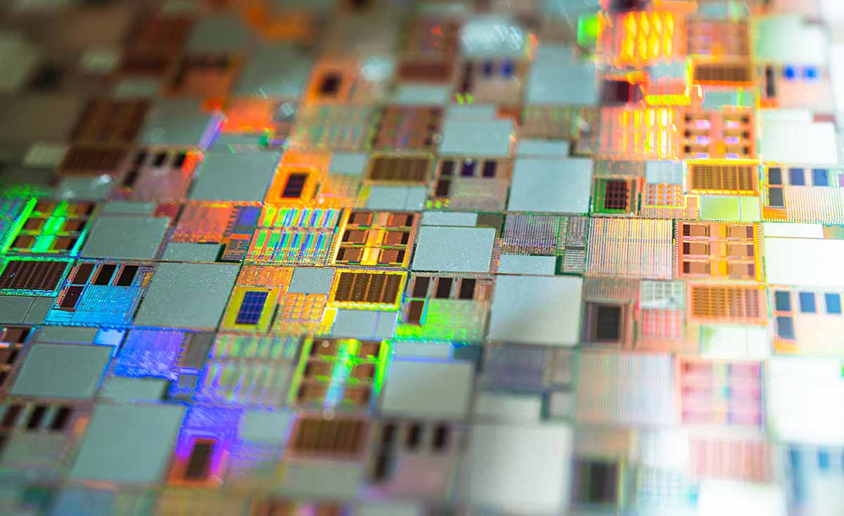
Omega Optical delivers essential photolithography, inspection, and metrology solutions to the semiconductor manufacturing market. Photolithography uses high-precision lenses and mirrors to transfer intricate patterns onto silicon wafers, with advanced DUV and EUV techniques achieving the fine resolution needed for modern chips. Inspection and metrology employ optical tools like microscopy and scatterometry to detect defects and ensure precision in wafer quality. Optical metrology, using ellipsometers and reflectometers, measures critical properties such as film thickness and refractive index, optimizing manufacturing processes and ensuring consistent semiconductor performance.

Semiconductor Applications

Application
Inspection, Machine Vision & Metrology
Application
Sensing and Illumination/ Plasma Monitoring
Application
Lithography
Application
Microscopy
Exploring Industry 4.0 and Application Capabilities

Industrial Optical Filters for Process Control

We are currently living through a major shift in industrial thinking. This is mainly focussed on the digitization of manufacturing processes, which is – in turn – based on greater automation and interconnectivity. You might have heard of Industry 4.0. The catch-all term used to describe a revolutionary paradigm shift affecting virtually every facet of industrial processing. At Omega Optical, we’ve witnessed this continued change through our industrial optical filters business.

News & Events

Project Info

Category: